1. reverse engineering
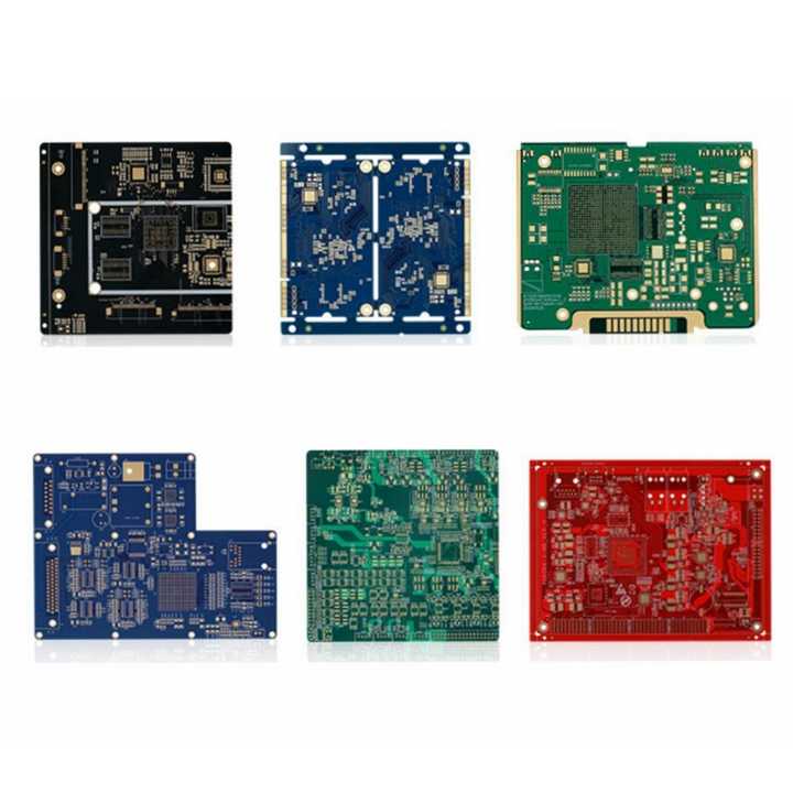
Reverse engineering a PCB (Printed Circuit Board) involves analyzing and reconstructing an existing circuit board to understand its design, functionality, and manufacturing process. This practice is used to recreate PCB schematics, layouts, and component arrangements, often to repair, analyze, or improve existing designs. It is a critical process in industries ranging from electronics manufacturing to product development and research.
Key Steps in PCB Reverse Engineering:
- Physical Examination:
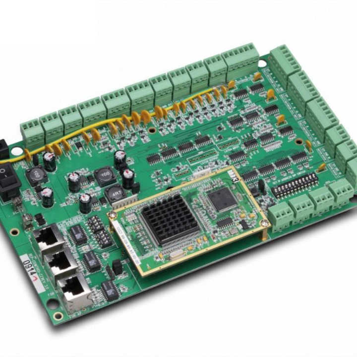
The reverse engineering process begins with a thorough visual inspection of the PCB. Key elements like the board’s layers, components, solder joints, and traces are analyzed to understand the general design. - Component Identification:
Each electronic component on the PCB is identified, including resistors, capacitors, ICs, transistors, and connectors. Part numbers and specifications are noted to find datasheets and understand their functions in the circuit. - Tracing Connections:
Electrical connections, such as traces, vias, and ground planes, are traced to map out the pathways between components. This step often requires specialized tools like continuity testers or circuit tracers. - Layer Mapping:
Multilayer PCBs require layer mapping to understand how internal layers are routed. Advanced tools such as X-ray machines or de-lamination techniques may be used to analyze hidden layers. - Schematic Reconstruction:
Using the data gathered, a schematic diagram is recreated. This step helps in understanding the logical flow of the circuit and its overall design. - Digitization:
The physical PCB layout and schematic are digitized using CAD software, such as Altium Designer, Eagle, or KiCad. This enables modifications, simulations, or reproductions of the PCB. - Documentation and Analysis:
The final step involves documenting the reconstructed design, analyzing its performance, and identifying areas for improvement or optimization.